Authors
Veronika Lin, Kelly Woo, Professor Srabanti Chowdhury
Abstract
Doping, or introducing impurities to an element or substrate, has been proven to be useful for modifying the conductivity of the finished product. Through ion implantation, precise doping can be achieved. Using the SRIM/TRIM Program, ion implantation was simulated to test different variables, including energy, depth, angle, as well the element or compounds making up the substrate or dopant. The investigation tested the energy against the depth, as well as testing different dopant and substrate species, and analyzing how the different species affected the depth of the ion and the damage done to the substrate. The results of this investigation confirmed that energy and depth have a direct relationship, while the mass of the ion and the depth have an inverse relationship, and that the substrate damage depends on the substrate species. The exact nature of the inverse relationship between the mass of the ion and depth as well as the relationship between the substrate species and the substrate damage must be further investigated.
Semiconductors, such as silicon, play an important role in the field of electrical engineering, serving as the basis of transistors, tiny devices that work to form everyday technological marvels such as computers and phones. The crystalline structure of semiconductors allows impurities to be introduced through a process called doping. Doping changes the properties of the semiconductors, allowing for increased conduction of electricity as the doped semiconductor will have more free carriers, electrons or holes, than a non-doped semiconductor. Doping enables more complex electronic devices to be designed and fabricated, such as diodes and MOSFETs, which circuits today are composed of. Through ion implantation, a dopant species is ionized and accelerated into the semiconductor. This method of doping allows for more control in where the implants are placed, which may enable better or more complex device designs.
Semiconductors1, with a high resistivity and a relatively small gap between the valence and conduction band, allow for the movement of free electrons between the valence and conduction band. However, semiconductors with wide bandgap have more recently been a popular topic of research. As opposed to silicon which has a bandgap of 1.12eV, wide bandgap semiconductors have band gaps >2eV. They exhibit higher carrier mobility, higher breakdown voltages, and some have better thermal conductivity as well. These properties allow wide bandgap semiconductor devices to function at higher frequencies, remain reliable at high temperatures, handle higher power more efficiently, and allow for smaller components which reduce noise and vibrations. Three of the more widely-known wide band gap semiconductors are gallium nitride, silicon carbide and diamond.
We propose to investigate ion implantation with target substrates of silicon, as well as the wide bandgap semiconductors, gallium nitride, silicon carbide, and diamond. We will compare the effects of implantation energy, dose, target material, and dopant species on the depth and concentration of the dopants and the damage created in the target. This will be done using a computer simulation program Stopping and Range of Ions in Matter (SRIM). SRIM, widely used in research, allows us to analyze these effects without doing in person experimentation. SRIM is a software that is based on the Monte Carlo algorithm.2 At its core, it is a random sampling based model that allows for the incorporation of uncertainty into the result. The algorithm, first used in atomic bomb calculations and testing in the 1940s and 50s, can be utilized for a wide variety of subjects, and in our case is used to simulate ion implantation by simulating many trajectories of single ions implanted into the bulk substrate. The usage of random sampling simulates the results of a real experiment with many trials and a selected number of runs.
Methods and Materials
The experiment was fully conducted using the SRIM software in order to simulate ion implantation with different dopants and substrates.
The relationship between the implantation energy and the depth of the ions was seen through data tables and graphs generated by SRIM. The implantation energy was varied through the changing of the energy value in the program. In order to exaggerate the resulting depth of each energy level, five runs ranging from 100 KeV to 500 KeV were performed at an incidence angle of 0 degrees, instead of the usual 7 degrees. Each run was performed once using 1501 ions to simulate the ion implantation procedure in order to ensure the runs were performed within the time constraints in order to reserve enough time to interpret the results while preserving the integrity of the results. Throughout the experiment, antimony and silicon were used as the respective dopant and substrate. Antimony was chosen as the dopant as a column 5 element and a n-type dopant to silicon, a commonly used substrate in electronics.
The program was also able to perform the simulation on different dopant and substrate species; both dopant and substrate could easily be changed through selecting the preferred dopant and substrate. In order to use a compound substrate consisting of multiple elements, another element could be added under the substrate section. By changing the dopant species while keeping the energy, angle and substrate constant, the difference in depth can be seen in an isolated setting. Six dopants were tested throughout the experiment — 3 p-type and 3 n-type dopants — with a constant substrate of silicon. Similarly, changing the substrate species while keeping other variables constant, the effect of the individual substrate can be seen in the depth in an isolated setting. Three substrates (silicon, silicon carbide and diamond) were tested against a single, constant dopant (nitrogen). For both investigations, 1500 ions were used to simulate the implantation in order to balance time constraints with precise results.
Results
Depth vs. Energy for Antimony in Silicon (100 KeV to 500 KeV)

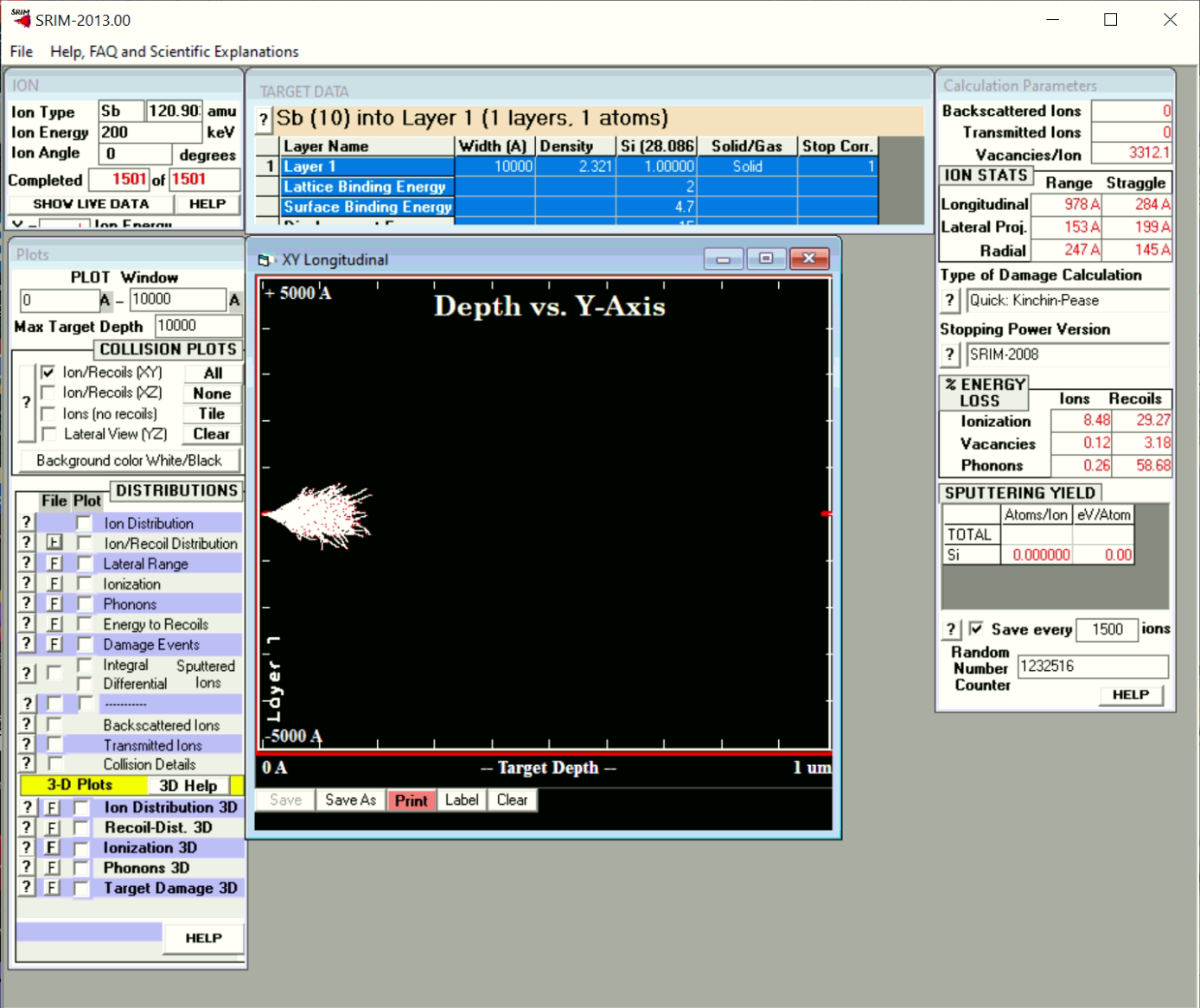


Figure 1: Through the automatically generated graphs, it can be seen that as the energy increased, the depth of the ion also increased — the white lines, representing the ion path, registers a higher value in the x-axis with each increase in energy, indicating a direct relationship between the energy and the depth.

Figure 2: The average range (or depth) of each run was plotted against the energy, resulting in a direct, linear relationship.

Figure 3: The average lateral range and radial range was plotted against the energy, also resulting in a linear relationship — demonstrating not only that depth and energy have a direct relationship in a one dimensional sense but in all three dimensions. Clearly, it can be seen that not only do energy and depth have a direct relationship; as the energy increases, so does the depth.

Figure 4: The ion depth of the three p-type dopants can be seen through the graph. The location of the peak of each curve on the x-axis represents the depth of the majority of the ions. The taller, narrower gallium peak represents more ions concentrated in one area in the substrate, while the shorter, more spread out peaks of aluminum and boron demonstrate a wider distribution of ions throughout the substrate.

Figure 5: The ion depth of the three n-type dopants can be seen through the graph. Figure 5 parallels Figure 4 with the heavier ions having a shorter range and the lighter ions having a longer range. The heaviest ion, arsenic, also has the highest peak, much like gallium in Figure 4. It was seen that the mass of the ion had an inverse relationship with the depth. The data demonstrates that the energy and depth have a direct relationship and can be seen through comparing the average range of the ions at 100 KeV to the average range of ions at 500 KeV. The average range of the ions at 100 KeV was 560.8 angstroms, while the average range of the ions at 500 KeV was 2200 angstroms. As the ions with the most energy had the most force applied, these higher energy ions would require more force to stop. The inverse relationship of the mass of the ion and the depth can be seen through Figures 4 and 5. Comparing the depth of the ion with the largest atomic number and therefore atomic mass with the ion with the smallest atomic number and smallest mass, it can be deduced that the atomic mass and depth have an inverse relationship. Arsenic, with an atomic number of 33 and an atomic mass of 74.922, had an average range of 1349 angstroms, while boron (Figure 4), with an atomic number of 5 and an atomic mass of 10.81 had an average range of 5694. As the ion’s atomic mass increases, the depth decreases.
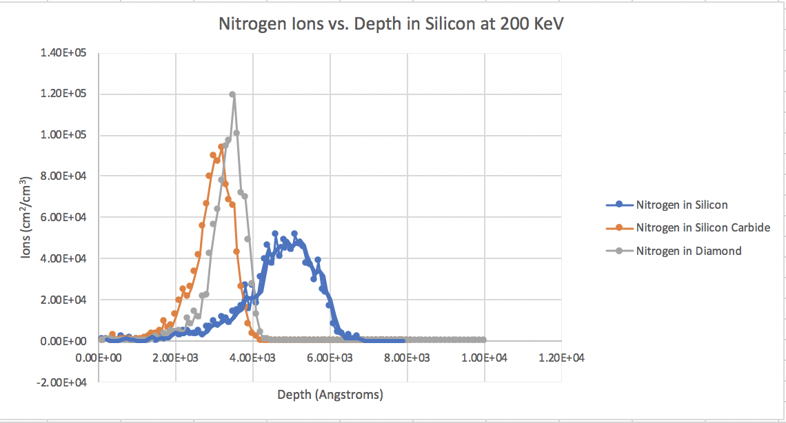
Figure 6: The graph illustrates the depth of nitrogen ions implanted in different substrates — silicon, silicon carbide and diamond. The relationship between the different substrate species and depth can be seen through the graph; clearly, even with the same, constant dopant, different substrate species affect the depth of the ion.

Figure 7: The graph illustrates the nitrogen ion damage in the silicon carbide substrate. The damage done to the silicon carbide can be broken down into the two individual elements making up the silicon carbide — silicon and carbon. It can be seen that silicon was damaged more — more silicon atoms were displaced when the nitrogen was implanted.

Figure 8: The graph demonstrates the displacement of both silicon and carbon atoms much like Figure 7; however, Figure 8 illustrates the other two runs of silicon and diamond. As seen before, silicon was displaced and therefore damaged far more than carbon. Through the graphs, it can be seen that the silicon substrate and carbon diamond substrate’s damage is significantly different. It can therefore be observed through the data that damage differs depending on the substrate.
Conclusion
The results of this investigation confirmed that energy and depth have a direct relationship, while the mass of the ion and the depth have an inverse relationship, and that the substrate damage depends on the substrate species. Energy and depth have a linear relationship with range equaling 4.091(range)+156.1, with an r-squared value of 1. The exact nature of the inverse relationship between the mass of the ion and depth as well as the relationship between the substrate species and the substrate damage must be further investigated.
Future Directions
For future experiments using SRIM and TRIM to simulate ion implantation, the number of ions tested should be as high as possible in order to obtain the most precise results. By increasing the number of ions, the simulation will take longer to run and should be run overnight. Other related experiments include the formation of the box profile. By varying the energy of runs, then transforming the data and multiplying by a common factor, a box profile can be constructed. A box profile can be useful as seen in CoolMos™ devices.
Acknowledgments
This investigation into ion implantation using SRIM would not be possible without Kelly Woo, Professor Srabanti Chowdhury and the rest of the Wide-Bandgap Lab. I would like to thank them for their hard work and their support of this experiment. I would also like to thank Cindy Nguyen and the STEM to SHTEM program for making this opportunity possible.
References
[1] The Potential of Wide-Bandgap Semiconductors. (n.d.). Power Electronic News. https://www.powerelectronicsnews.com/the-potential-of-wide-bandgap-semiconductors/
[2] Monte Carlo Simulation. (n.d.). https://www.goldsim.com/web/introduction/montecarlo/